Intel is revitalizing its presence in Santa Clara, the heart of Silicon Valley, by establishing a new chip manufacturing facility on its Bowers Avenue campus. This move signals a significant shift after years where the company’s industrial expansion primarily focused on locations like Arizona, Oregon, New Mexico, Ireland, and Israel, rather than its historic California base. While not a traditional chip fabrication plant (FAB), this new facility plays a crucial role by supplying essential materials to the aforementioned locations, thereby enhancing their production capabilities.
The project, though not massive in scale, is a potent initiative for producing semiconductor wafers. It is specifically designed to strengthen a vital component of the chip manufacturing chain: the masks used in the printing of chip designs. This reinforces Intel’s commitment to returning manufacturing to its foundational site in Santa Clara, aiming to equip its FABs with improved performance for chip production.
The announcement was made public by prominent Intel figures, Pushkar Ranade and Ashish Tuli, who shared details of the groundbreaking ceremony, emphasizing Intel’s return to chip manufacturing in Santa Clara. Ranade, a key figure within the company, serves as Chief Technology Officer and Chief of Staff to CEO Lip-Bu Tan, overseeing technological strategy, special projects, and emerging technologies such as quantum computing, photonics, and neuromorphic computing.
Tuli, as Corporate Vice President and Head of Corporate Development, focuses on strategic initiatives, corporate operations, and investments. The joint announcement from these high-ranking executives underscores Intel’s gradual but steady resurgence in financial and manufacturing strength.
The official city documents identify the project as BW2 + CUB2 at 3065 Bowers Avenue. Intel plans to construct a three-story manufacturing building alongside a Central Utility Building on approximately 2.4 acres in the southwest corner of its existing campus. The technical documentation outlines a total of 101,971 square feet, comprising 77,533 square feet dedicated to manufacturing and 24,438 square feet for the utility building.
This facility will house cleanrooms, manufacturing support spaces, tool servers, electrical equipment, storage areas, security systems, chillers, cooling towers, pumps, piping, process water, process air, and emergency generators. In essence, Intel is constructing a fully functional industrial component with all the necessary technical infrastructure to support this critical part of the manufacturing process.
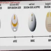
Crucially, the city acknowledges that Intel plans to manufacture masks for chip processing. While this might not sound as glamorous as producing CPUs or GPUs, it is fundamental to the entire semiconductor creation process. These highly precise masks act as templates, transferring chip designs onto wafers during lithography. By bolstering this capability in Santa Clara, Intel is directly reinforcing its advanced manufacturing efforts and its commitment to regaining industrial prominence in the United States. The hope is that this resurgence will lead to greater competitiveness, offering consumers better products at more affordable prices.