
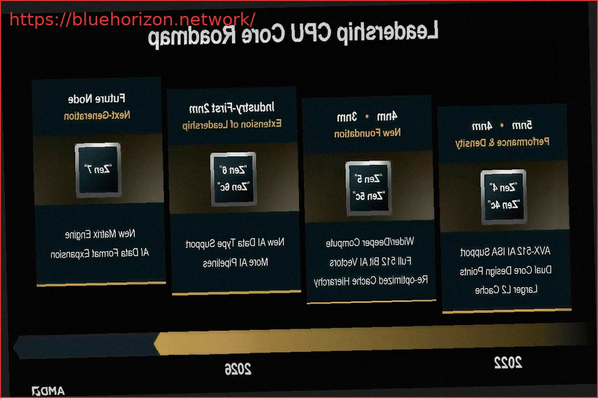
AMD is reportedly already planning its next significant advancements beyond Zen 6, pointing directly towards Zen 7. According to information from Commercial Times, the AMD Zen 7 architecture, with its CCD codenamed “Grimlock,” is expected to leverage TSMC’s A14 node. This refers to a future 1.4nm manufacturing process from the Taiwanese foundry. The projected release window is 2028.
A key aspect of this news is that AMD is not only looking at a new lithography node but also at a substantial change in packaging. The reports mention FOPLP, or Fan-Out Panel-Level Packaging. This design is said to be developed in collaboration with Powertech Technology (PTI). This packaging approach allows for larger panels to be utilized instead of relying solely on the traditional format of circular wafers, which can help reduce costs and improve scalability for highly complex designs. For Zen 7, this would be logical given the discussions of larger CCDs, more cores, increased cache, and new variants featuring 3D V-Cache.
What We Know About the AMD Zen 7 Architecture
The most striking detail is that future AMD Zen 7 CCDs could feature a configuration of up to 16 cores per chiplet. This is a significant departure from the 8 cores per CCD that AMD has traditionally used in its modern desktop Ryzen processors. Furthermore, variants with 3D V-Cache could potentially offer up to 224 MB of L3 cache per CCD, a massive increase compared to current X3D models (96 MB). TrendForce also corroborates earlier rumors suggesting 2 MB of L2 cache per core, 4 MB of L3 cache per core, support for FP512, integrated AI acceleration directly within the CCD, and an estimated IPC improvement of 15% to 25% over AMD Zen 6.
The A14 node information aligns well with TSMC’s public roadmap. TSMC itself introduced A14 as its next major logic node after N2, with mass production anticipated for 2028. According to official data, A14 is expected to offer up to 15% higher speed at the same power consumption, or up to 30% lower power consumption at the same speed, along with over a 20% improvement in logic density compared to N2. This makes the leak highly plausible. If Zen 6 is already associated with TSMC N2, then Zen 7 on A14 would represent a logical evolution for a generation expected around 2028.
The official context further supports the idea that AMD is aggressively pursuing more advanced nodes and packaging. Recently, AMD confirmed that its upcoming EPYC Venice processors are already in production on TSMC’s N2 node in Taiwan, with plans to also move production to TSMC Arizona. AMD described Venice as the industry’s first HPC product to enter production on TSMC’s advanced 2nm process.
The Leak Follows AMD’s Investment in the Taiwanese Ecosystem
Additionally, AMD announced last week over $10 billion in investments within the Taiwanese ecosystem. This funding is specifically aimed at strengthening advanced packaging, interconnect, and manufacturing capabilities for AI infrastructure. This official announcement mentions technologies like EFB 2.5D, collaborations with ASE, SPIL, and PTI, and the validation with PTI of the first FOPLP-based EFB 2.5D interconnect. While not a direct confirmation of FOPLP for Zen 7, it clearly indicates that AMD is preparing a supply chain where advanced packaging will be as critical as the lithography node itself.
In essence, this leak paints a picture of a significantly more ambitious AMD Zen 7 than a mere IPC improvement. The architecture appears poised to combine three key advancements: a much more advanced TSMC A14 node, chiplets with higher core density, and more aggressive 3D caching. For desktop use, this could pave the way for Ryzen CPUs with more cores without abandoning the chiplet approach. For EPYC servers, it would enable increased density, cache, and efficiency per socket. And for AI/HPC, advanced packaging will be crucial for connecting chiplets, cache, memory, and interconnects with lower power consumption and higher bandwidth.
Fundamentally, this information suggests that AMD is already securing its place in the supply chain for a CPU generation that is still some time away. AMD Zen 6 will be the immediate next step, with Venice for servers and likely its consumer equivalents. We are talking about the AMD Ryzen 10000 and Ryzen AI 500 series, further down the line. Zen 7, however, is targeted for the latter half of the decade and will depend on various factors: the actual maturity of the A14 node, costs, initial yields, TSMC’s capacity, the availability of advanced packaging, and AMD’s commercial strategy against Intel and Arm.