IMEC, which in 2023 had positioned the leap to atomic transistors as a much nearer goal, expecting to be below the nanometer mark with A2 around 2036 and an evolution based on GAA, FSFET, CFET, CMOS 2.0, and BSPDN, has updated its roadmap. This previous roadmap aimed to explain how CPUs, GPUs, and AI accelerators would continue to gain density as traditional scaling approached its physical limits. Unfortunately, IMEC’s updated roadmap for 2026 presents a significantly more challenging timeline, pushing these advancements beyond 2041.
The new roadmap alters the schedule and dampens initial enthusiasm, leading to more extended node lifecycles and increasingly distant target dates. Consequently, as anticipated with the general slowdown in technological progress, improvements will become more incremental, and atomic transistors are now expected closer to mid-century rather than the present.
IMEC Unveils 2026 Roadmap with Major Corrections: Has Lithography Slowed Down Permanently?
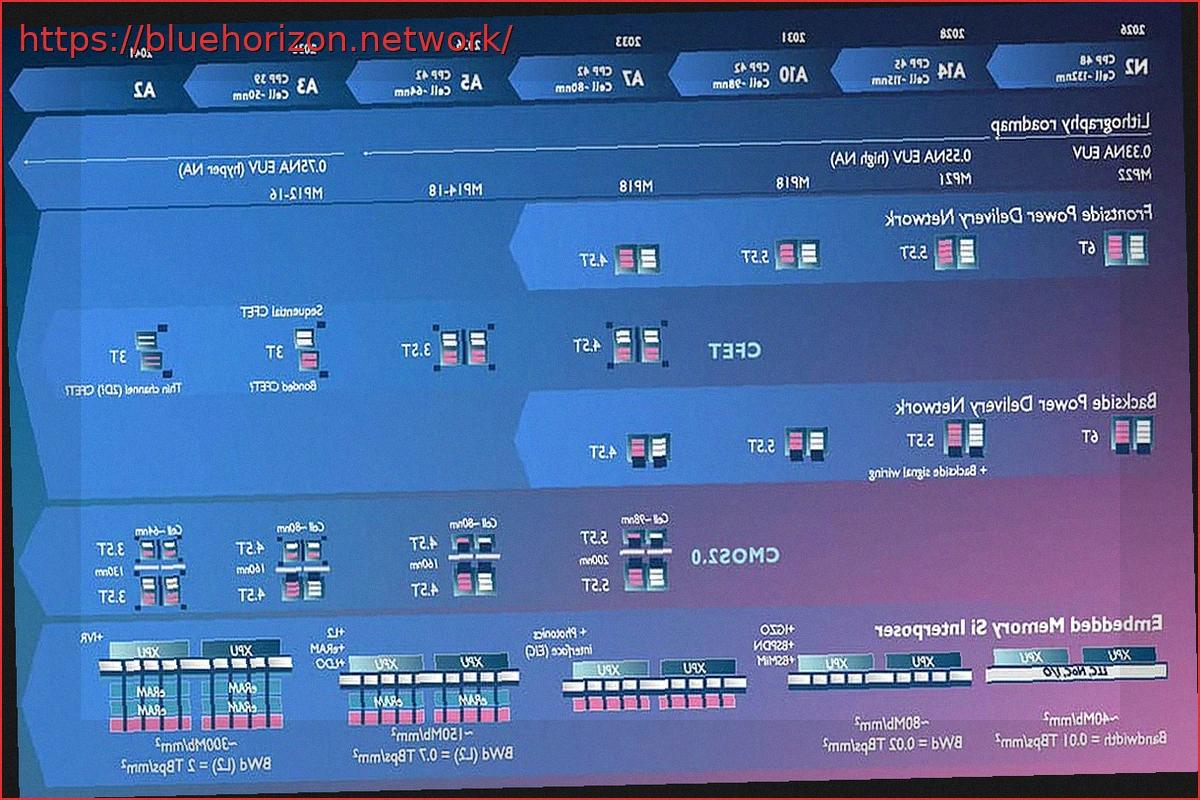
Indeed, A2, referring to 2 Angstroms (not 2 nanometers), which was envisioned as the disruptive cornerstone, is no longer slated for 2036 but for 2041. The path to achieving this is now spread across various nodes, lithography advancements, power delivery solutions, CFET, CMOS 2.0, and integrated memory on silicon interposers.
In terms of nodes, IMEC starts with N2 in 2026, featuring a Contacted Poly Pitch (CPP) of 48 nm and a cell size of approximately 132 nm. This is followed by A14 in 2028, with a CPP of 45 nm and a cell size of about 115 nm. A10 is expected in 2031, with a CPP of 42 nm and a cell size of approximately 98 nm. A7 is planned for 2033, maintaining a CPP of 42 nm and reducing the cell size to around 80 nm. A5 is set for 2036, with a CPP of 42 nm and a cell size of about 64 nm. A3 appears in 2038, with a CPP of 39 nm and a cell size of roughly 50 nm, while A2 is now slated for 2041 without any additional specified features, which is somewhat unusual.
Lithography advancements will accompany this progression. The N2 node will utilize 0.33 NA EUV, while EUV High-NA with 0.55 NA will be introduced from A14 in 2028 and continue for the next decade. Subsequently, EUV Hyper-NA with 0.75 NA will pave the way towards A3 and A2. The Metal Pitch will also decrease from MP22 to ranges like MP12 or MP16, indicating that merely changing the transistor design is insufficient; significant compression of metallic layers is also required. Therefore, it’s possible that A2 may also be introduced without specific advancements in this area.
Regarding Frontside Power Delivery Network (FPDN), power will continue to be supplied from the front of the chip, following a traditional approach. However, IMEC is progressively moving from 6T designs to 4.5T, as each generation offers less space for transistor power delivery and signal routing on the same face. Furthermore, FPDN’s limitations are expected to be reached by 2033 with A7, as further reductions will not be possible with GAA, necessitating a shift to CFET.
Embedded Memory Si Interposer, the Key for AI from TSMC, Intel, and Samsung
With Backside Power Delivery Network (BSPDN), power delivery is shifted to the rear of the chip. This frees up the front side for critical interconnections. Additionally, the roadmap includes backside signaling from A14, a technology already seen with TSMC and available from Intel. Within CMOS 2.0, under the BSPDN architecture, the final stage shows cell sizes of approximately 64 nm by 2041 with A2, integrated into more advanced designs. It is also noteworthy that A2 will feature Thin Channel technology.
Finally, and of significant importance, is the Embedded Memory Si Interposer (EMSI). This technology transforms the interposer into a far more active component. It progresses from approximately 40 Mb/mm² and 0.01 TB/s/mm² to around 300 Mb/mm² and 2 TB/s/mm², incorporating IGZO, BSPDN, BSMiM, photonic interfaces, L2, eRAM, LDO, and IVR. Consequently, the future of CPUs and GPUs will be a convergence of advancements in transistors, power delivery, memory, and advanced packaging, though not at the previously anticipated pace.
As IMEC’s 2026 roadmap demonstrates, the technological stagnation in chip evolution and architecture has been significantly impacted. The upcoming steps will be not only less pronounced but also stretched over a much longer duration. Therefore, the **transition of transistors presents the most significant challenge**, as the shift from GAA to CFET completely bypasses Forksheet and atomic scaling. Moreover, this process is extended by a considerable five years, an eternity in this sector. In light of this, Moore’s Law suffers another setback, with no fundamentally new transistor types emerging, and CMOS 2.0 appears to be the primary hope for continued progress.