
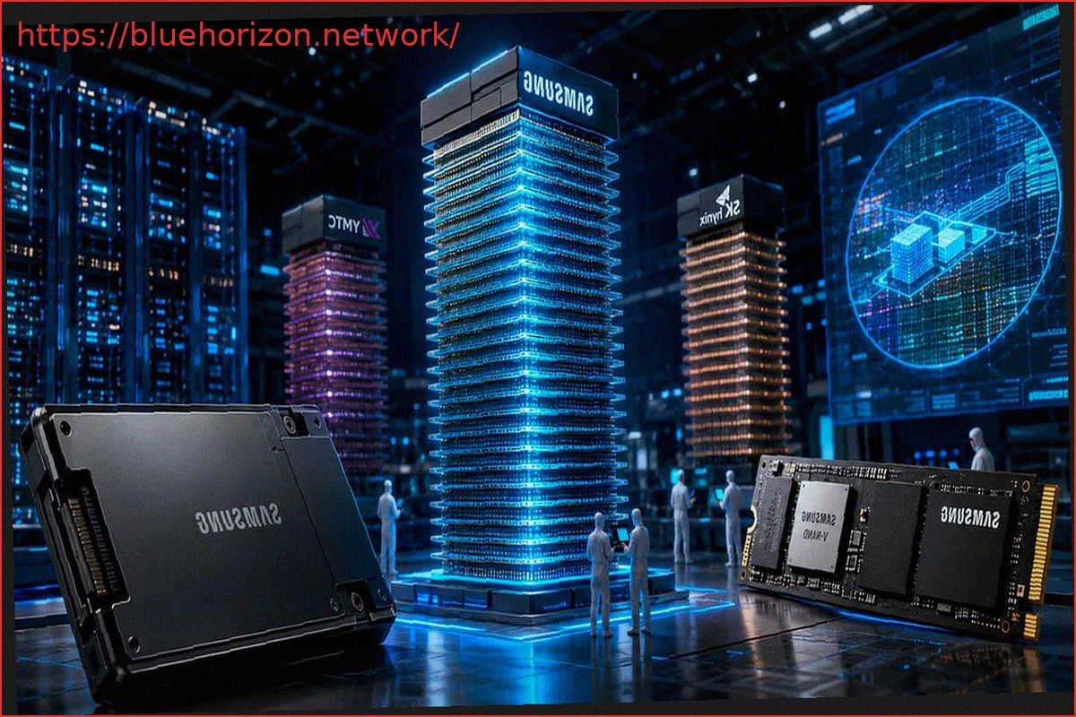
Samsung has reportedly completed the development of a functional prototype of 900-layer 3D NAND memory, a major technical advancement in the pursuit of increasing storage chip density. According to South Korean media, the company has achieved this by combining two 450-layer NAND structures using a technology called Cell Multi Bonding (CMB). Crucially, this isn’t just a lab mockup; Samsung asserts that normal operating characteristics of the memory cells have already been verified.
The core concept is straightforward to explain, though incredibly complex to manufacture. Instead of solely stacking layers vertically in a single structure, Samsung has joined two 450-layer NAND memory blocks to form an equivalent 900-layer structure. This brings the company much closer to the symbolic goal of 1,000-layer NAND, a benchmark the industry has been striving for years to increase SSD capacity without solely relying on shrinking cell sizes.
However, the first SSDs with Samsung’s 900-Layer 3D NAND Memory Will Take Time to Arrive
The primary challenge is that the taller the NAND layer stack becomes, the more difficult manufacturing, alignment, and reliability become. To achieve this prototype, Samsung had to overcome two key hurdles: wafer deformation, known as warpage, and microscopic alignment errors during the bonding process. They reportedly utilized an advanced Upper Chuck design for holding and stabilizing the wafer, along with new overlay correction technology to enhance layer precision.
Improvements in bitline and wordline structures, essential for reading and writing data within NAND memory, are also mentioned. Theoretically, these changes could reduce both power consumption and the final chip size, which is critical if Samsung aims to integrate this technology into data center SSDs, AI servers, and, eventually, higher-capacity consumer drives.
Based on the information, Samsung has achieved a research prototype, not a mass-production-ready NAND memory. Given the current trend of NAND memory being directed towards data centers, servers, and AI, it’s clear Samsung will want to bring this technology to market as soon as possible. There’s no better time than the present, with the AI boom, for this memory to further break its current records in both revenue and profit.
First, We’ll See V10 NAND Memory with a Design Exceeding 400 Layers
In summary, Samsung has developed a research prototype, not 3D NAND memory ready for mass manufacturing. When this memory becomes a reality, it is expected to enable the creation of SSDs with up to 983TB of capacity. In the short term, Samsung is already working on its future V10 NAND. As far as is known, it will be above 400 layers and target speeds of 5.6 Gbps per pin. This generation would be a more realistic intermediate step before reaching commercial products with 900 or 1,000 layers.
Currently, rivals like SK Hynix have already begun producing 321-layer NAND, one of the highest figures known in commercial production. On the other hand, Chinese company YMTC is aggressively pushing chips with over 300 layers. In the best-case scenario, this would mean Samsung could enable SSDs up to 160TB. SK Hynix could enable SSDs up to 246TB, and YMTC up to 246TB as well. Everything will depend on the exact number of layers and whether TLC or QLC memory is used.
This memory will first arrive where it matters most: data centers and AI servers. In the consumer market, these advancements will take longer to materialize and will allow for the creation of higher-capacity SSDs. However, high capacity is logically suited for this market, as high-density drives are primarily intended for enterprise and AI applications.